Skip to content
Integrated photonics · Advanced packaging

Photonic devices and packaging for AI semiconductors

from materials to systems

AI 반도체 광통신Co-Packaged Optics집적광학

CPO: 광 송수신 소자를 AI 칩과 같은 패키지 안에 집적해 전기 배선의 대역폭·전력 한계를 넘는 기술

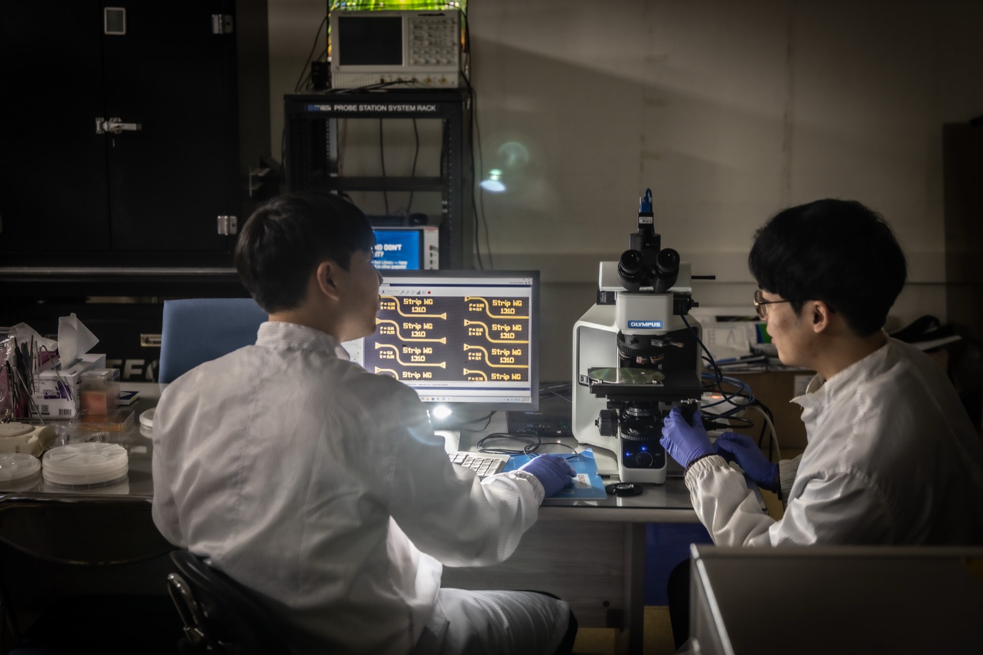
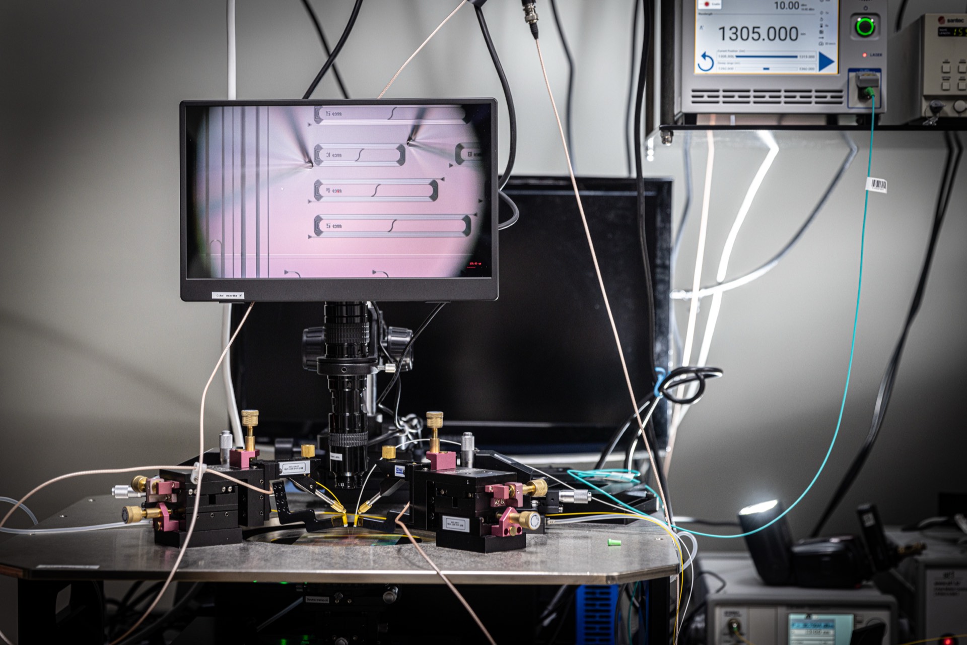
PIC inspection under an optical microscope (Jan 2026)
Featured research · SING

SiN-on-Glass: photonic devices and packaging for co-packaged optics

AI 가속기 간 데이터 전송은 전기 배선의 대역폭과 전력 한계에 직면합니다. 우리는 유리 기판 위 실리콘 나이트라이드(SiN) 플랫폼, SING에서 광소자를 설계·시뮬레이션하고 제작·측정하며, 이를 광·전기 하이브리드 패키지로 통합해 패널 레벨 광 재배선층과 CPO로 연결합니다.

AI chiplets linked by light on a glass panel Concept top view: two AI chiplets sit on a shared glass packaging panel, each next to a photonic engine. Three SiN waveguides on the glass carry light between the engines in both directions, and the receiving chiplet lights up when a pulse arrives. GLASS PANEL SiN waveguide AI AI PIC PIC
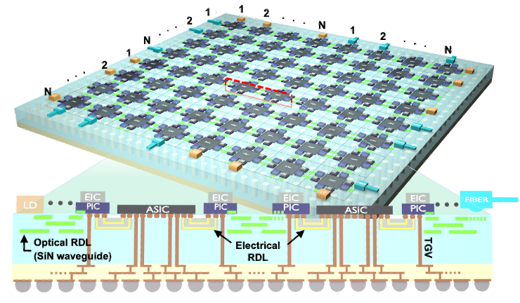
SiN-on-Glass panel carrying many chiplets, with a cross-section showing laser, EIC on PIC, ASIC, SiN optical redistribution layer, electrical redistribution layer and through-glass vias
SING glass-core package for optical and electrical hybrid integration (concept).
  • Optical RDLSiN waveguides on glass: low loss, high density, multilayer routing and high reliability across the panel.
  • PICSi photonic chips with high-speed optical modulators (MRM, MZM) next to each ASIC.
  • LD · SOA · SwitchLight sources, SOA integration and non-volatile optical switches for the optical network on glass.
  • Fiber-to-GlassOptical coupling from fiber into the glass panel with grating couplers (GC) and edge couplers (EC).
  • Glass-to-PICEvanescent couplers (EVC) between SiN-on-Glass and the Si photonic chip.

Materials

  • SiN on glasspanel-scale substrate
  • a-Si / SiNgrating layer · simulation
  • Bottom metal reflectorcoupling efficiency
  • Ferroelectric-oxide stacknon-volatile switching

Systems

More research

Si PIC modulators, next-generation memory and displays

Photonics · Si PIC

High-speed optical modulators for Si photonic chips

Ring and Mach–Zehnder modulators that turn electrical bits into O-band light, built on Si, SiGe and III-V/Si phase shifters for co-packaged optics.

III-V/SiSiGeMRMMZMO-bandPAM-4
Electronics · Ferroelectric memory

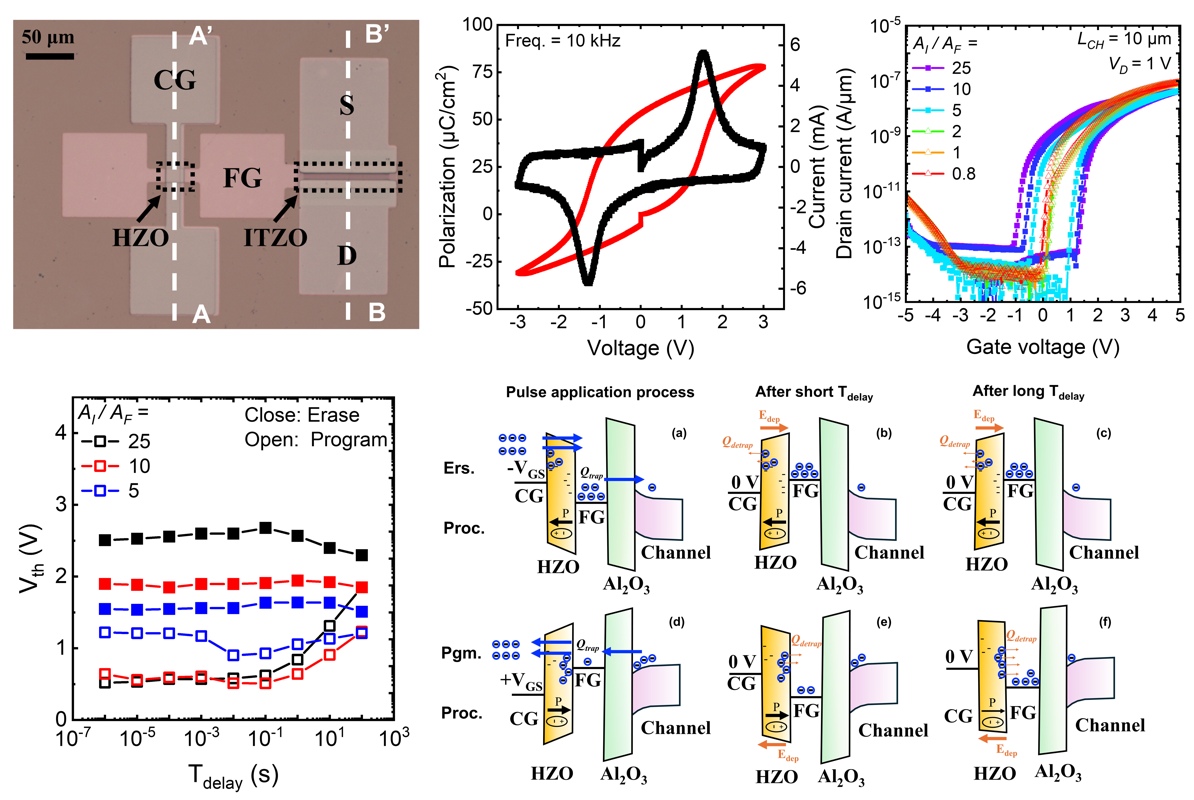
Ferroelectric transistors for non-volatile memory and in-memory computing

FeFETs and FeDRAM cells on amorphous oxide semiconductors, from switching dynamics and stability to computing-in-memory cells.

FeFETFeDRAMMFMISOxide semiconductorComputing-in-memory
Optoelectronics · Display

QD-LED and micro-LED pixels with memory-in-pixel backplanes

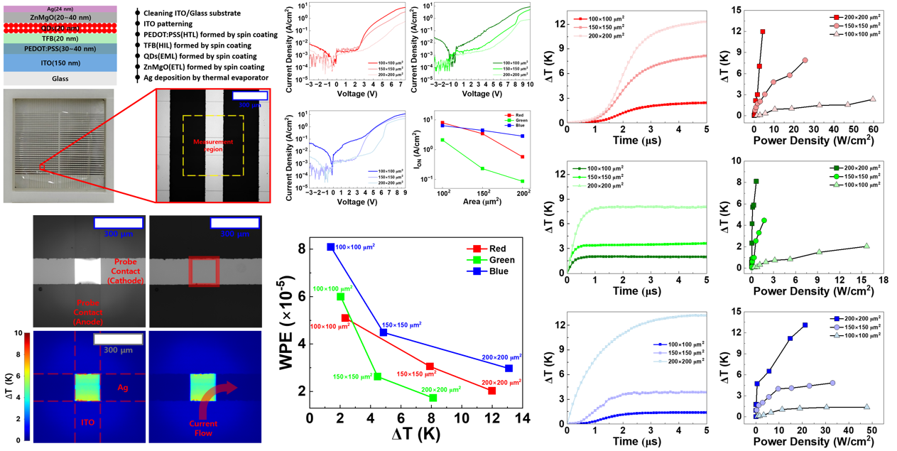
Charge-trap and ferroelectric oxide TFTs that hold each pixel's state, with thermoreflectance to map how the pixels heat up.

QD-LEDMicro-LEDMemory-in-pixelCharge-trap TFTThermoreflectance
Facilities

We design, fabricate and measure in-house

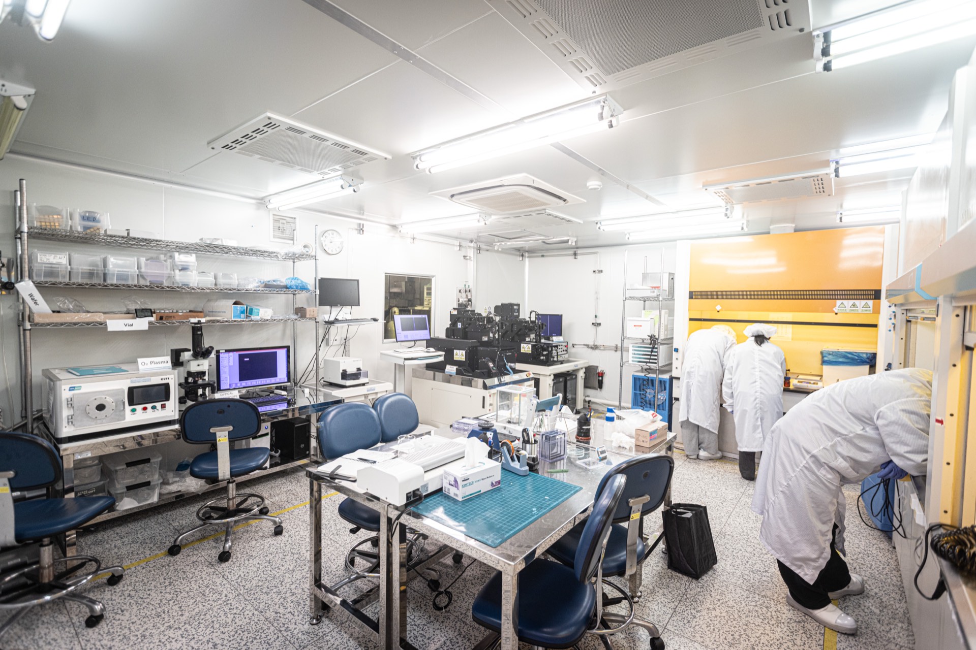
설계한 소자를 우리 클린룸에서 제작하고, 우리 측정실에서 바로 검증합니다.

ASDL cleanroom with lithography and inspection stations
ASDL CleanroomThin-film deposition, lithography, etching
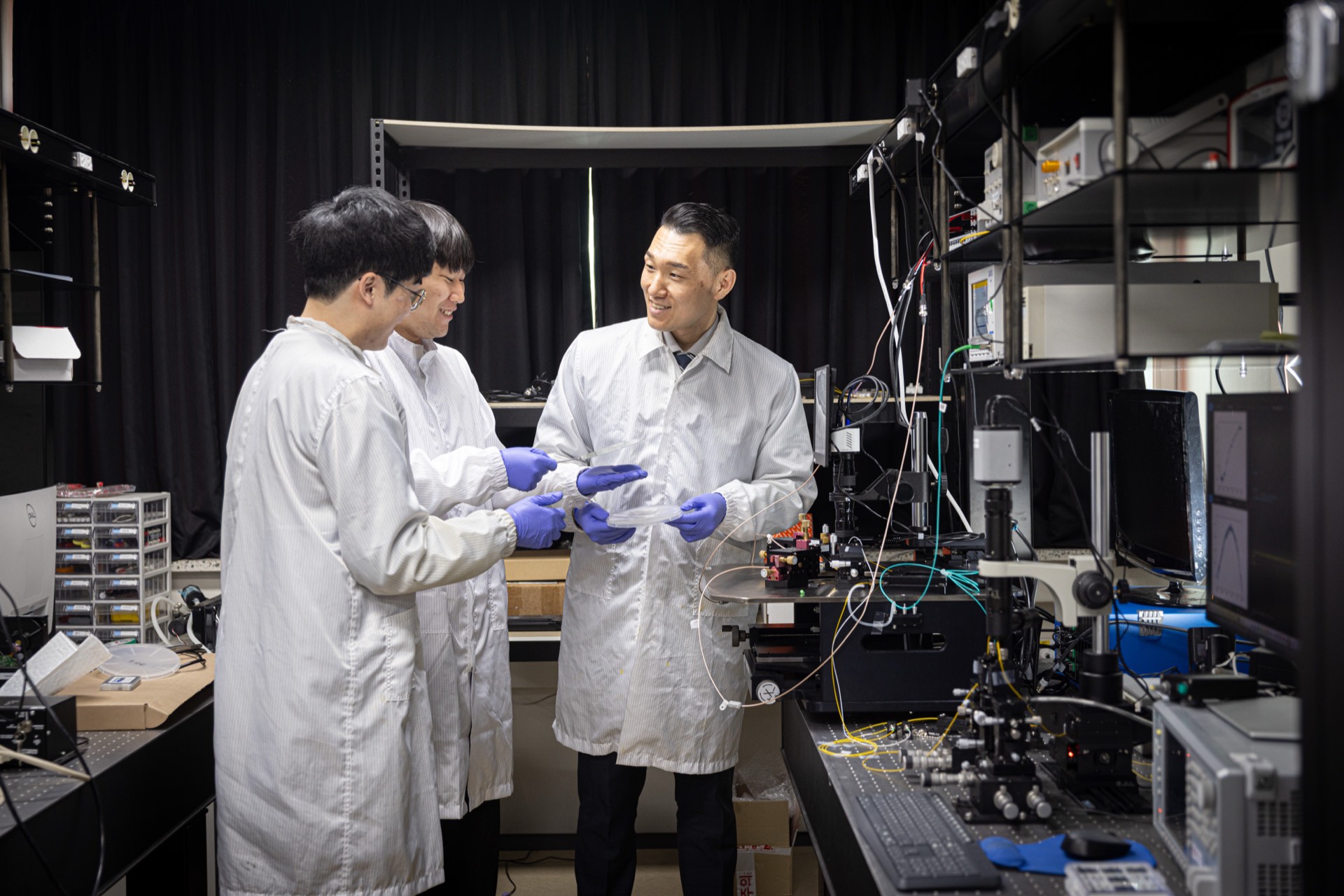
Fiber-coupled photonic chip on a probe stage with an O-band laser source
Photonic Device MeasurementFiber-to-chip coupling, O-band laser sources
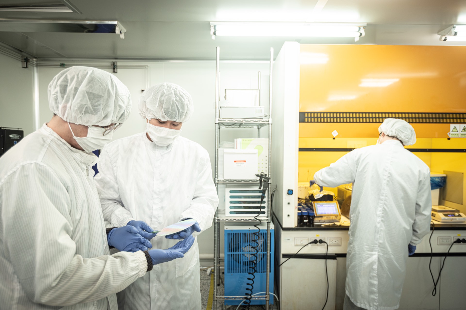
Two researchers inspecting a wafer under an optical microscope
PIC InspectionOptical microscopy of fabricated circuits
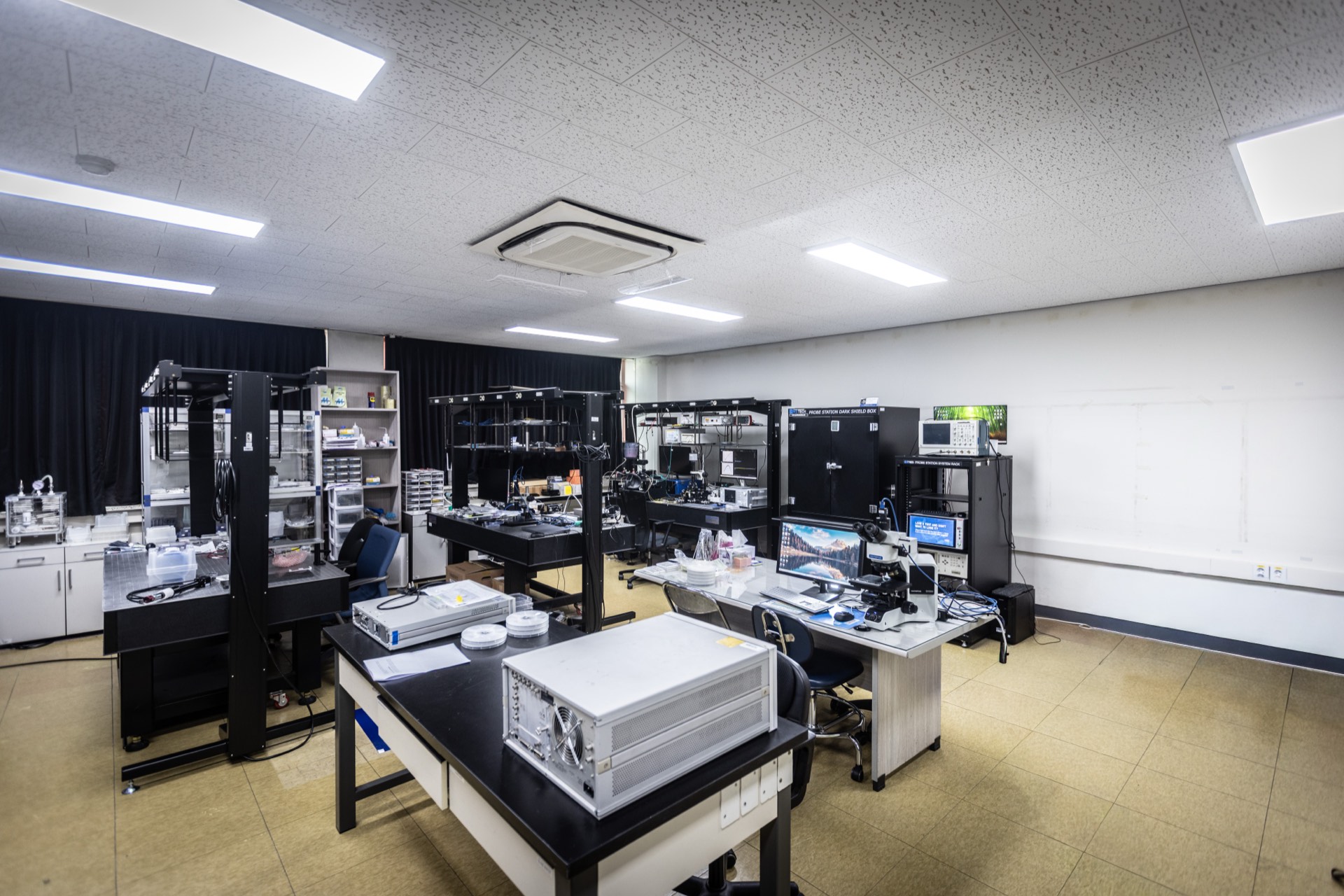
ASDL measurement laboratory with probe stations and instrument racks
Electrical & Optical LabProbe stations, parameter analyzers
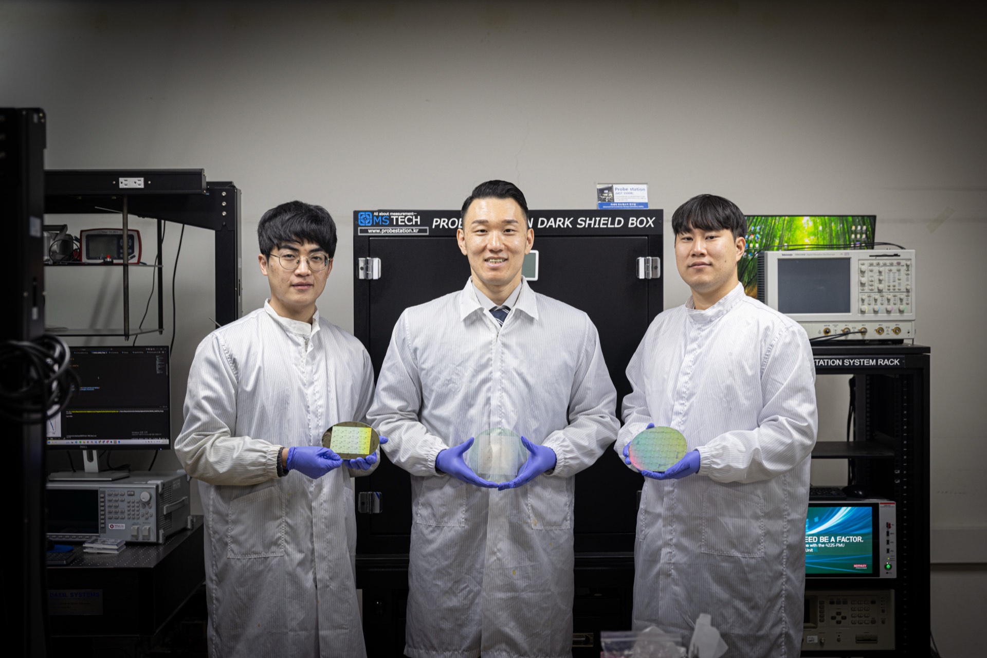
Researchers holding processed SiN-on-glass and silicon wafers
Wafer-level ProcessingSiN-on-Glass and silicon wafers
Join ASDL

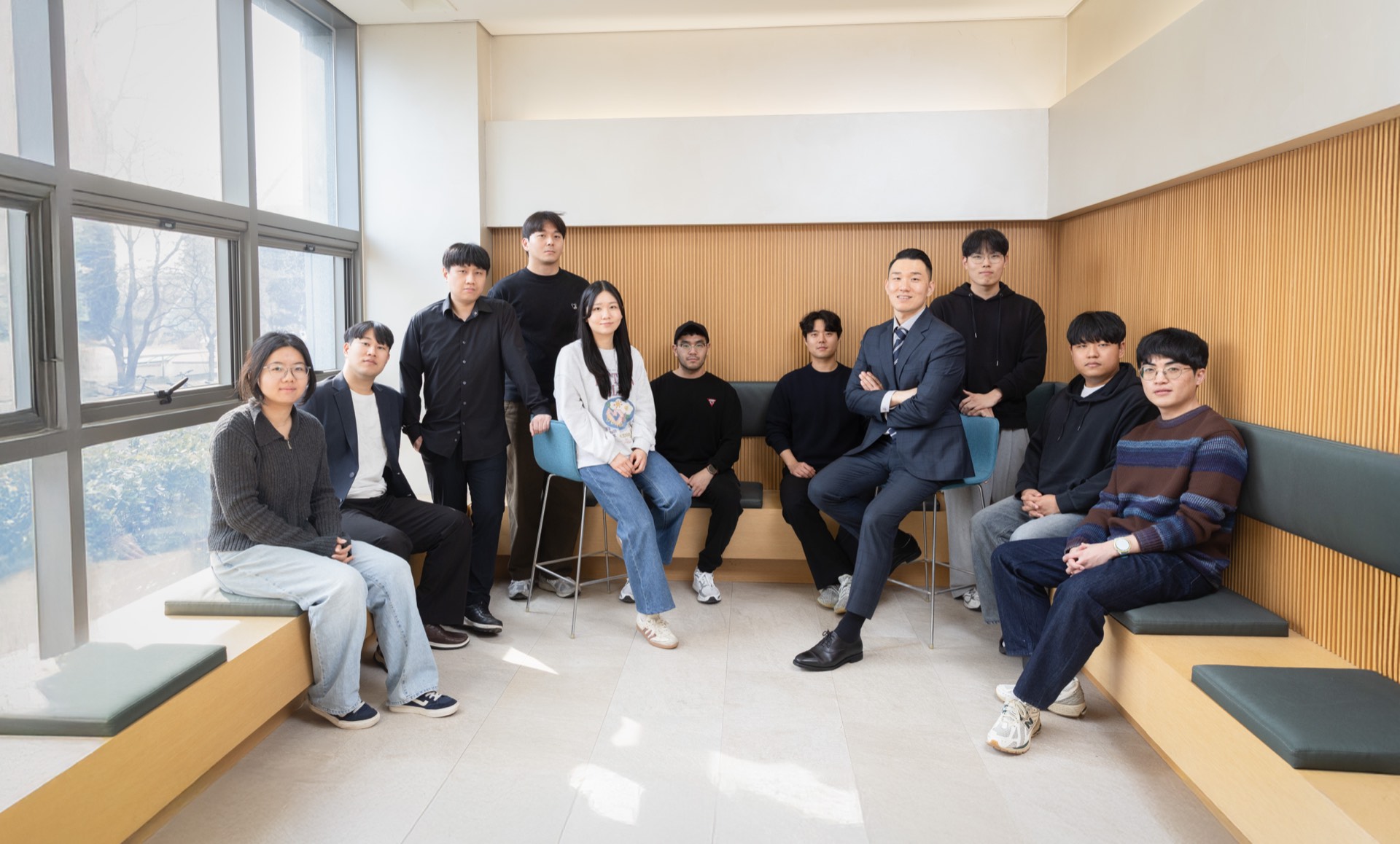
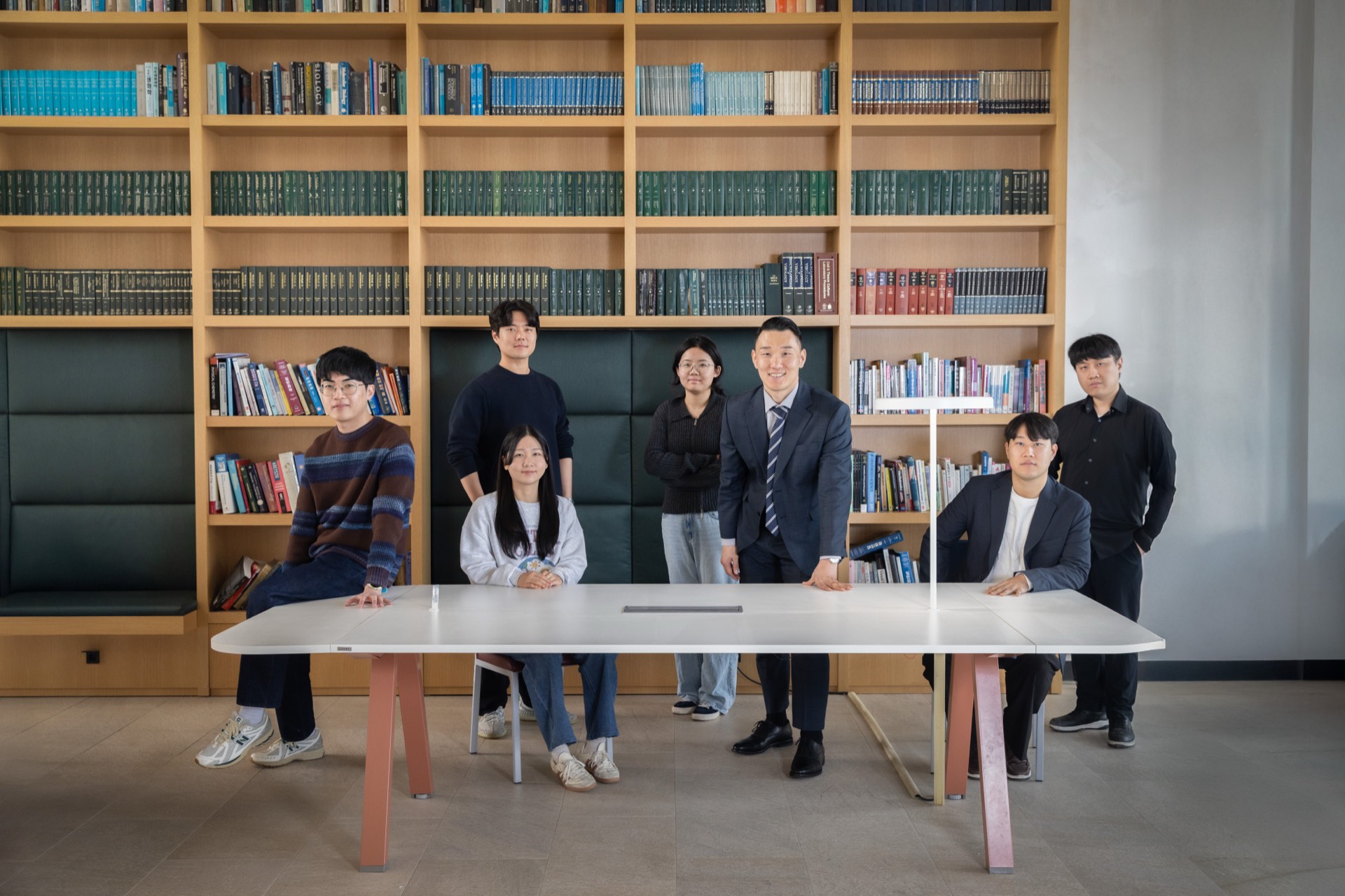
석사·박사 과정 및 학부 연구생을 모집합니다

광소자 설계부터 클린룸 공정, 광 측정까지 한 연구실 안에서 직접 경험합니다. 집적광학, CPO, 반도체 소자에 관심 있는 학생은 연락 주세요.

ProfessorYounghyun Kim · 김영현
Emailyounghyunkim@hanyang.ac.kr
LocationSchool of Semiconductor Convergence Engineering, Hanyang University ERICA, Ansan