Si-based optical modulators
IMEC, July ‘18 - present
- Device performance improvement
- Device modeling
- Device design optimization
Explore : III-V/Si MZ Modulator
IMEC, July ‘18 - present
We proposed the III-V/Si MZ modulator which is monolithically integrated on Si Photonics platfrom. Thanks to the superior electro-optic property of III-V materials, the device performance is expected to breakthrough the limited performance of conventional Si MZ modulators.
Selected paper
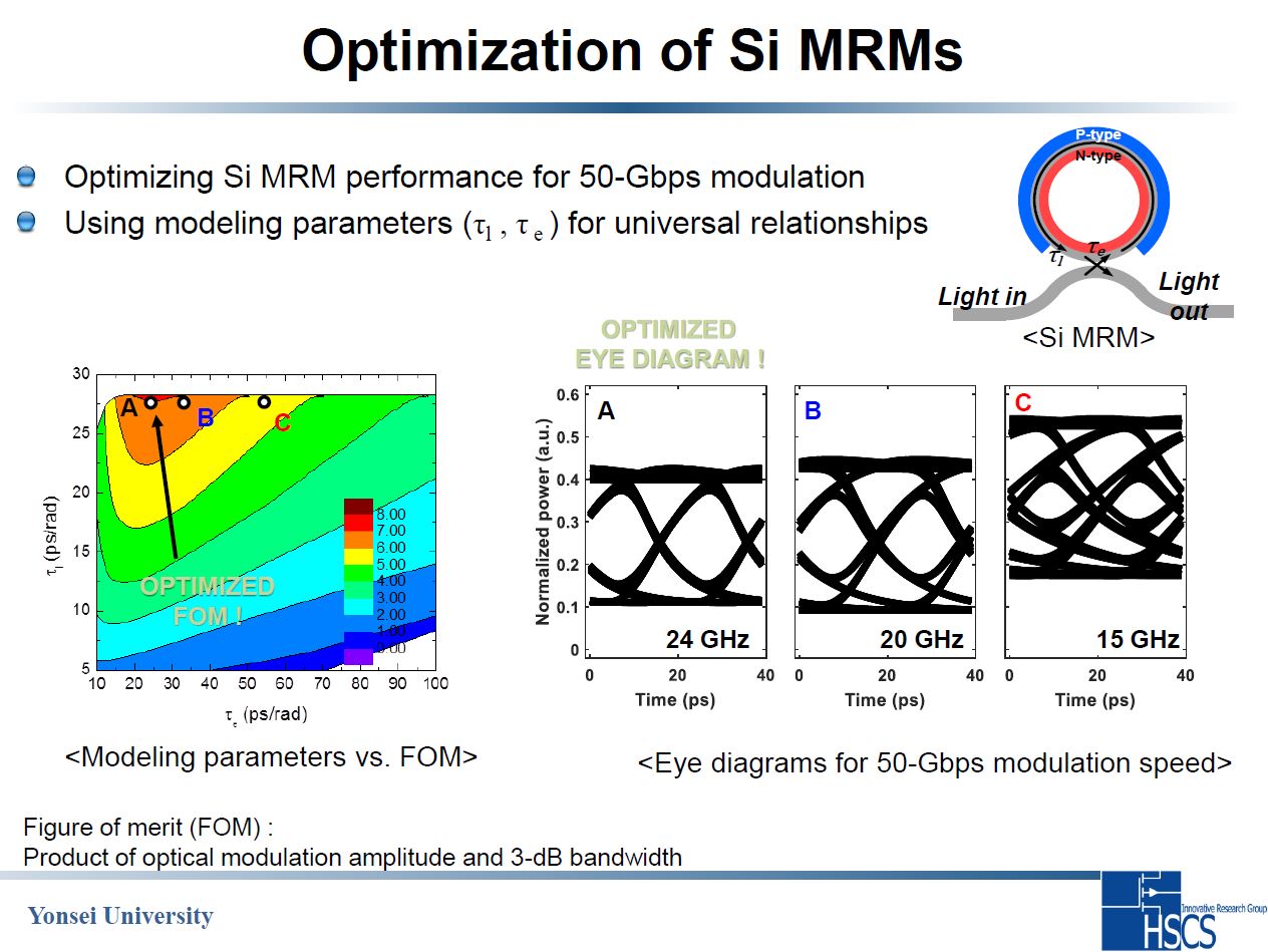
Systematic design guide for high-speed Si micro ring modulator
Yonsei Univ., Apr ‘17 - May ‘18
The Si micro-ring modulator is expected to play an important role in optical interconnect systems thanks to the large modulation bandwidth and small device footprints. There are many reports for analysis and experimental demonstrations. However, a systematic device design guide for determining optimal doping concentrations, ring radius, and coupling strength between ring and bus waveguides for a target data rate is not available. In this work, we study on realizing such a design guide.
Selected paper
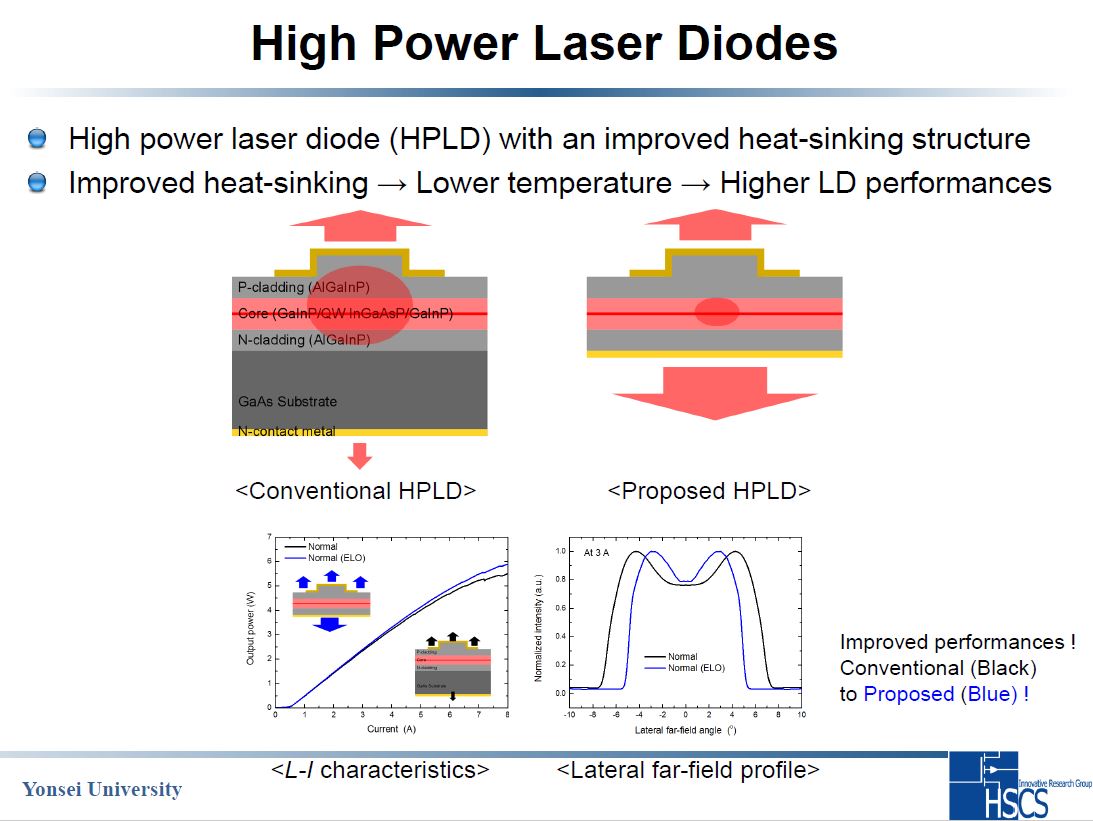
Numerical analysis on high-power laser diode
Yonsei Univ., Apr ‘17 - May ‘18
High-power laser diodes are highly attractive for material processing and military applications. However, the performance of a laser diode is easily deteriorated by thermal effect due to high-power operation; e.g. thermal lens effect which induces low beam quality. In this work, we numerically analyze the mechanism of the deterioration of laser diodes, and suggest the improved device structures.
Selected paper
Micro LED display
Seoul Semiconductor/Viosys Apr ‘15 – Mar ‘17
Micro LED is considered to be a key enabling technology for the next-generation display technology. Micro LED is based on inorganic materials, mainly GaN or GaAs, which is much more efficient than organic LEDs. However, it is difficult to package millions of micro LEDs for millions of sub-pixels of a display. In this project, we have demonstrated the packaging methods, micro-LED structures, and display structures.
- US20170287887A1, Display apparatus and manufacturing method thereof, Oct. 5 ‘17
- US20170250329A1, Display apparatus and manufacturing method thereof, Aug. 31 ‘17
- US20170250164A1, Display apparatus and manufacturing method thereof, Aug. 31 ‘17
- US20170194304A1, Display apparatus, Jul. 6 ‘17
- WO2017014564A1, Display device and method for manufacturing same, Jan 26 ‘17
- US20170025388A1, Display apparatus and manufacturing method thereof, Jan 26 ‘17
Strained SiGe optical modulator
Univ. of Tokyo Apr ‘10 – Mar ‘15
Silicon photonics is one of the most promising technologies for electronic-photonic integrated circuit. The Si optical modulator is a key component to encode electrical signals into light. However, the bottleneck of a Si optical modulator is low modulation efficiency due to weak electrooptical effects in Si. In this work, we introduced strained SiGe technology to boost the performance of a Si optical modulator, and successfully demonstrated as follows:
Selected papers
- Younghyun Kim et. al.,“Strain-induced enhancement of plasma dispersion effect and free-carrier absorption in SiGe optical modulators”, Scientific Reports 4, no.4683 (2014).
- Younghyun Kim el. al.,“Demonstration of record-low injection-current variable optical attenuator based on strained SiGe with optimized lateral pin junction,” Optics Express, Vol. 23, No. 9, p.12354 (2015)
- Younghyun Kim, Junichi Fujikata, Shigeki Takahashi, Mitsuru Takenaka, and Shinichi Takagi: “First demonstration of SiGe-based carrier-injection Mach-Zehnder modulator with enhanced plasma dispersion effect,” Optics Express, Vol. 24, No. 3, p.1979 (2016)

BTO-on-Si optical modulator
IMEC Aug ‘14 – Sept ‘14
The objective of this work is to improve the modulation efficiency of a Si-based optical modulator, in conjunction with Barium titanate (BTO). We numerically analyzed the device performance and optimized the device structure.
Graphene transistor
SAIT (SAMSUNG) Jul ‘13 – Aug ‘13
Graphene has attracted a lot of attention in recent years for the extremely outstanding physical properties. The main aim of this project is to investigate ozone cleaning effect on graphene for removal of PMMA residue.
GaN Power MOSFET
Univ. of Tokushima Sept ‘09 – Mar ‘10
GaN power transistors have the potential to reduce energy comparing to the conventional Si-based power transistors due to high breakdown voltage and speed switching. In this work, we demonstrated a GaN MOSFET with a silane-based SiO2 insulator by PECVD, which enables operation of 15-V gate voltage with ignorable leakage current.